Modern electronic devices use complex PCB or printed Circuit Boards as their backbone. With sophisticated and compact electronic systems the use of PCB board in usa, to accommodate the growing number of components and circuits in a limited space, has increased considerably. VLSI circuit and chip companies are crucial in advancing technology by developing high-performance, energy-efficient and compact integrated designs used in multiple electronic and automotive devices. Using printed circuit boards along with the VLSI circuits ensures these high-level chips are integrated into the functional electronic systems. The printed boards for circuits can be multi-layered in design and routing them requires skill and careful planning. With the right strategies to route them, you can achieve optimal performance and manufacturability.
The design for printed circuit boards requires creating intricate layouts that connect various electronic components while ensuring reliable signal integrity and power distribution. For high-speed applications, there is a need for advanced pcb design services to ensure precision, durability and performance. Combined with VLSI circuit companies, the firms designing PCBs in the U.S. enable the development of increasingly powerful and efficient electronic devices that are reliable and help shape modern industries. Let us look in detail at the various strategies for effectively routing complex and multi-layer designs in PCBs and the key considerations and practices used by the designers:
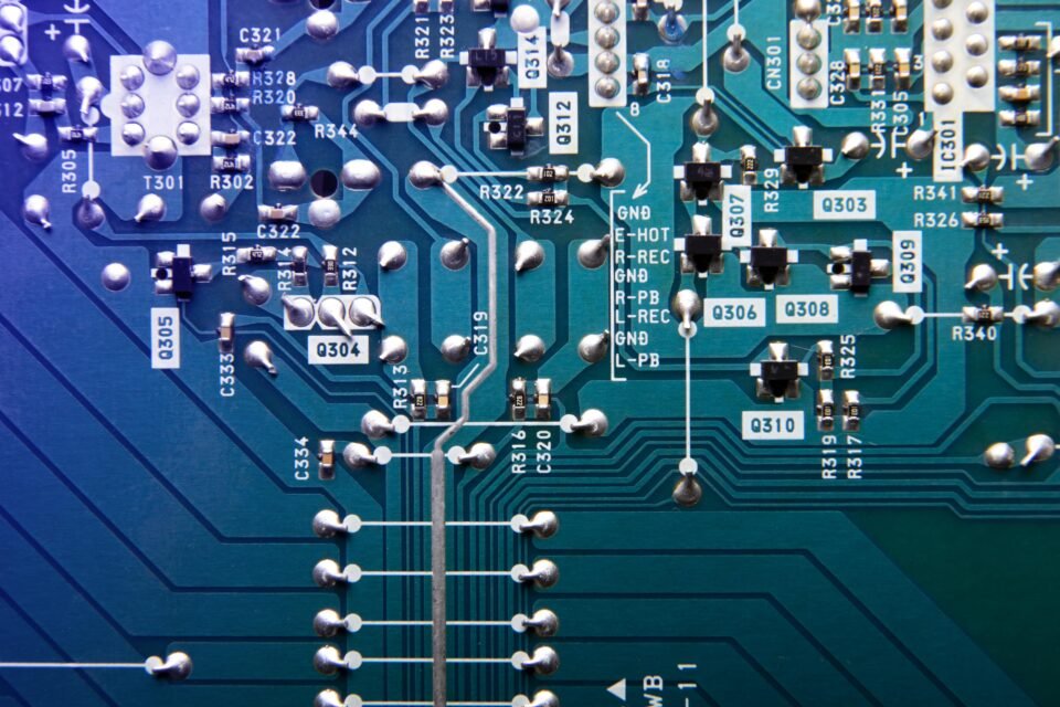
1. Understanding multi-layer PCBs:
One of the first steps in planning the multi-layered boards for routing requires understanding and knowing about the complex boards. This understanding is required as these boards have more than two layers of conductive material separated by insulated layers allowing for complex routing. This routing is essential to ensure that modern devices that run on high-density interconnects and compact designs can be routed to perform optimally. The layers in the boards are divided into separate parts for performing different functions, such as carrying data and signals, distributing voltage and maintaining signal integrity across the board. Efficiently routing these with minimal interference ensures optimal signal integrity. This requires careful planning and know-how of the PCB’s electrical and physical characteristics.
2. The importance of signal integrity:
A multi-layered design is chosen primarily to ensure signal integrity. The efficiency and clock speeds of the electronic components are increasing continuously. This necessitates a multi-layered design and routing of the PCBs for clean and free signals without interference. As various factors such as crosstalk impeding matching or grounding can contribute to the quality of signals and hinder its efficiency, there is a need to ensure that designers use a combination of proper grounding and controlled impedance traces along with careful routing to mitigate these risks. It helps to check the passing of signals from high-noise or high-power areas thereby affecting its quality and minimising trace length.
3. Layer stack-up planning:
When the multi-layered boards are designed, care is taken to include the various elements and arrangements of signal, power and ground layers. This is essential to ensure signal integrity manufacturability plus the overall performance of the PCB. Thus, proper planning for stack-up is the key strategy while designing a multi-layered board and must be kept in mind to minimize the efforts. Using ground planes helps to shield sensitive signal layers and reduce electromagnetic interference. There is a need to reduce the risk of warping so symmetry is maintained while designing the boards.
4. Advanced routing techniques:
Routing is a complex and technical task requiring advanced strategies and careful consideration. You can use the Via technology that can use holes to route between multi-layers of the boards or connect only the outer layer of the PCB to one of the inner layers. Alternately, the inner layers may be connected through vias without extending to the outer layers. Vias help design and connect the PCB layers to ensure optimum output. Further, the goal of routing is to minimize trace lengths and reduce complexity. This goal can be achieved by placing the components optimally and using two differential pairs for high-speed signals. Additionally, using power and ground planes makes routing efficient, serving as low-resistance paths for distributing power and minimizing noise. So these planes are placed adjacent to the layers. When high-current components are to be routed, it is essential to properly define the power and ground lines to minimize power loss.
5. Managing design rules and constraints:
Adherence to specific design rules and constraints ensures manufacturability and performance in routing multi-layered PCBs. The rules must be complied with for trace length and spacing to ensure proper signal transmission. The via sizes should be considered carefully to reduce the chances of oversized board space. Further, in complex designs, the heat dissipation in power-hungry components is also a concern that must be addressed.
6. Tools and software for routing:
The use of specialized tools and software for routing multi-layer PCBs is essential as these tools provide powerful features such as automated routing and design rule checks along with 3-D visualization of the board layout. This helps to identify potential issues in routing before actually implementing the plan by removing any obstacles in manufacturing and the risk of errors.
Conclusion:
It can be rightly concluded that with strategic planning and knowledge of electrical engineering principles, you can use advanced techniques to route complex multi-layered PCBs. However, to achieve the desired results, it is essential to consider using technology in signal integrity and layer stack-up. By using the best practices you can find advanced design solutions to ensure that the final product functions as expected while meeting the necessary manufacturability requirements. With the continuous advancement of electronics, the need to route the complex PCBs becomes critical. Only the expert designers will be well-positioned to drive innovation in the field and master the techniques. In advanced circuit boards where high-performance computing is required along with precision and durability, the required high-speed applications can give their best performance only with the latest designs and accuracy. The routing requires skill and precision to ensure optimum output with minimum effort and maximum efficiency. So when you are routing complex PCB designs, you must strategize for multi-layered boards to get the ideal results.